經典邏輯閘(上):電腦運算的基礎

作者:
林昱誠(Yu-Cheng Lin)
閱讀時間:
5
分鐘
# 經典邏輯閘(上) 在[入門系列文章](https://www.entangletech.tw/lesson/popular-02)與上一篇文章中,我們提到,電腦資訊的最基本單位是 bits(位元)。我們可以將數字、文字、符號、圖片與影片透過 bits 的狀態(0 與 1)表示(或說編碼)。在這一節中我們將介紹如何操作 bits 的狀態,以讓電腦進行「運算」。 我們會用所謂的 logic gates(邏輯閘)操作 bits 的狀態。Logical gate 的基本架構如下圖,資訊從左邊輸入進 gate,經過 gate 的轉換與操作後,從右邊輸出資訊
圖片內容

這邊舉個簡單但不精確的例子,假使有個 logical gate 叫加法閘,當我們將兩個「1」輸入這 gate,這 gate 會執行「1+1」的運算,並輸出「2」
圖片內容

為了清楚了解每個 logical gate 的操作規則,我們會列出所謂的真值表(truth table)。如下圖,表格的左邊是對 gate 輸入(input)什麼樣的資訊,右邊則是對應 gate 會輸出(output)的資訊。 \begin{array}{|c|c|} \hline \text{Input} & \text{Output} \\ \hline & \\ \hline & \\ \hline \end{array} 在接觸量子計算前需要先了解經典電腦邏輯閘的原因是,經典邏輯閘是現代數位運算的基礎,它們構成所有數位電路與電腦系統。初識它們的工作原理,能幫助你更好地理解量子邏輯閘(quantum gate),並將其應用於量子計算中。 以下我們將簡單介紹各種常見的邏輯閘 ## 常見的邏輯閘 ### Identity gate 又稱為 buffer gate。輸入 0 給 identity gate,輸出 0;輸入 1 則輸出 1,就是沒變。
半加法器

Identity gate 的電路圖

\begin{array}{|c|c|} \hline \text{Input} & \text{Output} \\ \hline A & Q=A \\ \hline 0 & 0 \\ \hline 1 & 1 \\ \hline \end{array} ### NOT gate 輸入 0 輸出 1,輸入 1 則輸出 0,NOT gate 的電路圖可以用下圖表示
半加法器

NOT gate 的電路圖

\begin{array}{|c|c|} \hline \text{Input} & \text{Output} \\ \hline A & Q=\overline{A} \\ \hline 0 & 1 \\ \hline 1 & 0 \\ \hline \end{array} ### AND gate 從這邊開始,gate 的輸入端有兩個,輸出端只有一個。在 AND(和) 中,只有兩個輸入都為 1 時,輸出才會是 1,否則都輸出 0。
半加法器

AND gate 的電路圖

輸出的結果相當於乘法 $A\cdot B$(你可以看到 0 乘任何數都是 0,只有 $1\cdot 1=1$) \begin{array}{|c|c|} \hline \text{Input} & \text{Output} \\ \hline A\quad B & Q=A\cdot B \\ \hline 0\quad 0 & 0 \\ \hline 0\quad 1 & 0 \\ \hline 1\quad 0 & 0\\ \hline 1\quad 1 & 1\\ \hline \end{array} ### OR gate OR 類似「或」的概念,只要有一個輸入是 1 就輸出 1,對應到二進位運算就類似「加法」(但不是真的加法)
半加法器

OR gate 的電路圖

\begin{array}{|c|c|} \hline \text{Input} & \text{Output} \\ \hline A\quad B & Q=A+B \\ \hline 0\quad 0 & 0 \\ \hline 0\quad 1 & 1 \\ \hline 1\quad 0 & 1\\ \hline 1\quad 1 & 1\\ \hline \end{array} ### XOR (Exculsive OR) gate 這個 gate 的操作原則就真的是(二進位)加法
半加法器

XOR gate 的電路圖

\begin{array}{|c|c|} \hline \text{Input} & \text{Output} \\ \hline A\quad B & Q=A\oplus B \\ \hline 0\quad 0 & 0 \\ \hline 0\quad 1 & 1 \\ \hline 1\quad 0 & 1\\ \hline 1\quad 1 & 0\\ \hline \end{array} ### NAND gate 在 AND gate 的輸出放上 NOT gate 就是 NAND gate,所以它的真值表就是把 AND gate 的輸出都做 NOT gate 處理
半加法器

NAND gate 的電路圖

\begin{array}{|c|c|} \hline \text{Input} & \text{Output} \\ \hline A\quad B & Q=\overline{AB} \\ \hline 0\quad 0 & 1 \\ \hline 0\quad 1 & 1 \\ \hline 1\quad 0 & 1\\ \hline 1\quad 1 & 0\\ \hline \end{array} ### NOR gate 跟上面的 gate 很像,就是 OR gate 後面接 NOT gate
半加法器

NAND gate 的電路圖

\begin{array}{|c|c|} \hline \text{Input} & \text{Output} \\ \hline A\quad B & Q=\overline{A+B} \\ \hline 0\quad 0 & 1 \\ \hline 0\quad 1 & 0 \\ \hline 1\quad 0 & 0\\ \hline 1\quad 1 & 0\\ \hline \end{array} ## 組成電路 有了以上介紹的邏輯閘後,就能透過這些邏輯閘做任何運算。像是以下這個由 XOR 與 AND 組成的半加法器(half adder)
半加法器

半加法器的電路圖

以數學形式來寫,即為 \begin{split} S&=A\oplus B\\ C&=AB \end{split} 要了解這個電路有什麼功能,一樣把真值表列出來 \begin{array}{|c|c|} \hline \text{Input} & \text{Output} \\ \hline A\quad B & C \quad S \\ \hline 0\quad 0 & 0\quad 0\\ \hline 0\quad 1 & 0\quad 1\\ \hline 1\quad 0 & 0\quad 1\\ \hline 1\quad 1 & 1\quad 0\\ \hline \end{array} 從表格中能看出這電路實現的功能為 A 與 B 相加,對應到十進制,即為 \begin{array}{|c|c|} \hline \text{Input} & \text{Output} \\ \hline A\quad B & A+B \\ \hline 0\quad 0 & 0\\ \hline 0\quad 1 & 1\\ \hline 1\quad 0 & 1\\ \hline 1\quad 1 & 2\\ \hline \end{array} 透過這些邏輯閘就能組出可以執行複雜運算的電路,這就是如今晶片之所以如此強大的原因 ## 如何實現邏輯閘 上面講了很多邏輯閘的原理,那麼在現實中,如何用實物來實現這些的邏輯閘操作呢?沒錯,就是現在當紅的「電晶體」,下圖展示了如何用電晶體與電線組成一個半加法器。
半加法器

以電晶體實現半加法器,紫色為輸入或輸出端,A 與 B 即為輸入端,sum 對應到上圖的 S,carry 則為上圖的 C;綠色為電晶體,藍色為電線
Picture come from B.,Srinivas(2013)

在實務上,晶片設計工程師會先討論這一代的晶片要具備哪些功能,並且這些功能如何用邏輯閘實現。接著,他們在 Verilog 或是 VHDL 上描述電路的結構與功能,像是下圖是用 Verilog 定義半加法器。 ```Verilog=+ module half_adder_structural ( input a, // 輸入 'a' input b, // 輸入 'b' output s, // 輸出 's' (Sum) output c // 輸出 'c' (Carry) ); xor gate_xor (s, a, b); // XOR gate for sum and gate_and (c, a, b); // AND gate for carry endmodule ``` 完成設計後,這些設計檔案會進行多次的驗證與模擬,確保設計無誤且符合需求。接下來,會透過電子設計自動化工具(EDA tool)將這些邏輯閘電路轉成電晶體的電路。
半加法器

利用 EDA tool 將半加法器的邏輯閘電路圖轉為電晶體圖

最後轉成晶片的佈局圖(layout),以供晶片製造商將晶片做出來。
半加法器

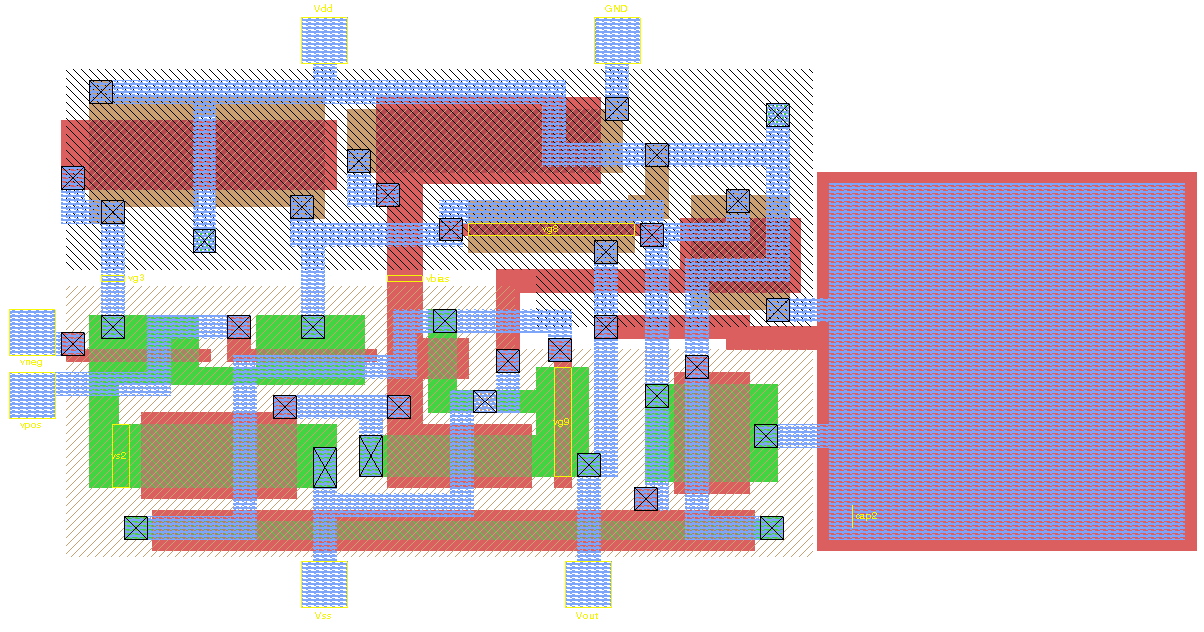
CMOS 運算放大器的 layout 圖,晶片製造商會根據這圖透過半導體工藝做出晶片
Picture come from wiki

上述只是簡單介紹晶片從設計到製造的簡要流程,實際上會比我們介紹得還要複雜

## 延伸閱讀 對於數位邏輯電路設計很有興趣的讀者,可以參看清華大學[數位邏輯設計線上課程](https://ocw.nthu.edu.tw/ocw/index.php?page=course&cid=230)
課程目錄